More results...

Early in the 20th century, the key component of electric devices was the vacuum tube. Vacuum tubes are devices that can control the electric current flow in a vacuum. When a voltage is applied vacuum tubes allow the current to flow in only one direction. These were the crucial part of early electric devices like radio, television, computers, etc. the disadvantages of vacuum tubes are, they were fragile bulky, and less efficient.
With the invention of PN junctions which are semiconductor devices in the 1940s, a new chapter began in electronics.
The most common semiconductor that is used to make p-n junctions. When semiconductors like silicon are supplied a voltage difference the electrons in the conduction band will move along the voltage.
Silicon atoms are arranged in a tetrahedral lattice. Between the atoms, there is a covalent bond that has two electrons. According to the molecular orbital theory, these electrons are in a molecular orbital. When a voltage is applied, these electrons travel into antibonding orbitals. In other words, electrons move from the valence band to the conductance band. So, the electrons in the conductance band are free to move. These free electrons are responsible for the current flow.
When electrons move from the molecular orbital, voids are created. These voids are called holes. These holes are not permanent and can be filled with another electron. Current flow in semiconductors depends on the number of holes and free electrons. If we can increase the number of free electrons or holes, the current flow can be increased. To increase the number of holes and electrons, dopants are added.
As mentioned earlier, the current flow of semiconductors depends on the number of holes and free electrons. To increase the conductivity of semiconductors, the number of holes or electrons should be increased. Doping is the process that adding impurities to a semiconductor structure, which will increase the number of free electrons or holes in the structure. So, the doping process increases the conductivity of the semiconductor.
the widely used semiconductor in the world today is Silicon. Silicon is doped with Boron, arsenic, phosphorus, and occasionally gallium. These are called dopants. These are elements in the 3rd or 5th group of the periodic table. According to the dopant, there are two types of doping.
When semiconductors are doped with an element that is in the 5th group of the periodic table, it will give an extra electron to the silicon matrix for each addition. Elements like phosphorus (P) have five electrons in their outermost shell. Semiconductors like silicon have four electrons in their outermost shell.
When silicon is doped with phosphorus, four electrons of phosphorus are acquired by four silicon atoms to make the eight electrons in their outermost shell. In this process, one electron out of five electrons of phosphorus is left without making a bond. In this type of addition, an extra negative charge is given to the semiconductor. Therefore, it is called an n-type or negative type of addition.

When silicon is doped with elements in the 3rd group of the periodic table like Boron it is called positive type or p-type addition. Each silicon in a pure silicon semiconductor is surrounded by four other silicon atoms. Boron has three electrons in its outermost shell. When Boron is doped with silicon, those three electrons will be acquired by three silicon atoms. One silicon atom is left without making a bond. Therefore, a positive hole will be created.

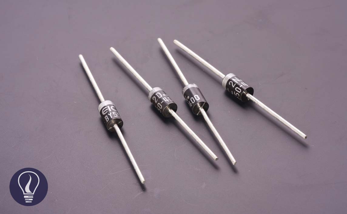
A p-n junction is created by doping group three elements and group five elements for two sides of the same intrinsic semiconductor. Therefore, it will form both n-type and p-type regions are formed on two sides of the same semiconductor. A p-n junction is formed at the center where p-type and n-type regions meet.

As soon as the p-n junction formed, the free electrons in the n-type region diffuse to the p-type region across the junction. Holes in the p-type region are filled with electrons. Here, positive holes are created in the n-type region. Due to the diffused electrons, a negative layer is created in the n-type region. Due to the positive and negative charge, a potential layer is created at the center of the semiconductor. This layer is known as the depletion layer. The depletion layer repels the impending charge carriers to diffuse. Therefore, this layer is called a potential barrier.
In silicon p-n junctions the potential barrier is 0.7 V. When it is used Germanium (Ge) the potential barrier will be 0.3V.
Biasing is applying a potential difference across the p-n junction using an external electric source. Biasing is two types as forward and reverse according to the direction of the external voltage.
The positive terminal of the external electric source is connected to the p-type region and the negative terminal is connected to the n-type region of the PN junction. Free electrons in the n-type region are repelled towards the junction by the negative potential.
At the same, holes in the p-type region are repelled by the positive potential. Therefore, the depletion layer narrows down. When the external potential exceeds the potential barrier across the junction (in silicon p-n junction potential barrier is 0.7V) a current flow occurs through the junction.

Here, the positive terminal of the external electric source is connected to the n-type region, and the negative terminal is connected to the p-type region of the p-n junction. In this case, free electrons are attracted to the positive terminal, and positive holes are attracted to the negative terminal. Therefore, the depletion layer is being broadened. Here, no current flow occurs.


The cover image was created using an image by zhuangwei500 from Pixabay